- Flex PCB Blog
- PCB Assembly Blog
- FPC Research Blog
- Preparation of FPC based on ultrasonic spraying method_4_Experimental Results
- Preparation of FPC based on ultrasonic spraying method_3_Experimental Procedure
- Preparation of FPC based on ultrasonic spraying method_2_Experimental Platform and Principle
- Preparation of FPC based on ultrasonic spraying method_1_abstract
- Research on Layout Design Method of Ultra-thin FPC_4_Analysis of Layout Design Methods
- Research on Layout Design Method of Ultra-thin FPC_3_Analysis of Layout Design Methods
- Research on Layout Design Method of Ultra-thin FPC_2_Analysis of Layout Design Methods
- Research on Layout Design Method of Ultra-thin FPC_1_introduction
- Research progress on polyimide FPC_2_the field of FPC
- Research progress on polyimide FPC_1_Introduction
- Analysis of Vibration Characteristics of FPCBs _4_Summary
- Analysis of Vibration Characteristics of FPCBs _3_Finite Element Analysis
- Analysis of Vibration Characteristics of FPCBs _2_Theory of Vibration Analysis
- Analysis of Vibration Characteristics of FPCBs Under Random Vibration_1_Introduction
- Design Methods for FPCBs_5_Practical Application
- Design Methods for FPCBs_4_Electrical Circuit Design and Examples
- Design Methods for FPCBs_3_Structure Design Method and Examples
- Design Methods for FPCBs_2_Component Selection Methodology and Examples.
- Research on Design Methods for FPCBs
- Application of MPW technique for FPCBs _4_Summary
- Application of MPW technique for FPCBs_3_Experimental results
- Application of MPW technique for FPCBs_2_Experimental setup
- Application of MPW technique for FPCBs_1_Principle of MPW
- Application of FPCB in PC motherboards_4_ Results and discussion
- Application of FPCB in PC motherboards_3_ Numerical analysis
- Application of FPCB in PC_2_ Experimentation
- Application of FPCB in PC motherboards
- A Bus Planning Algorithm for FPC Design _4_Experimental result
- A Bus Planning Algorithm for FPC Design _3_Proposed Algorithm
- A Bus Planning Algorithm for FPC Design _2_Preliminaries
- A Bus Planning Algorithm for FPC Design _1_Introduction
A Bus Planning Algorithm for
FPC Design in Complex Scenarios_1_Introduction
Abstract--Flexible printed circuit(FPC) design in complex scenarios has a list of pin concentration areas, which lead to extremely congested intersection regions while connecting the pins.Currently,it is challengingto explore the routability and to find topologically non-cross-ing and routable paths manually for the nets timely. The existing bus planning methods cannot offer optimal solutions concerning the special resource distribution of FPC design.To investigate an effective way to shorten the routing time of FPC and achieve enhanced performance, a bus planning algorithm is proposed to tackle complex area connection problems. On the basis of the pin location in- formation, the routing space is partitioned and generally represented as an undirected graph, and the topological non-crossing relationship between different regions is obtained using the dynamic pin sequence. Considering the routability and electrical constraints, a heuristic algorithm is proposed to search the optimal location of the crossing point on the region boundary. Experimental results on industrial cases show that the proposed algorithm realize better performance in terms of count and routability in comparison with numerous selected state-of-the-art router and methods.
I. Introduction
As one of the promising techniques of the printed circuit board (PCB), flexible printed circuit (FPC) has been widely used to connect components in three-di- mensional (3D) space. In particular, FPC is capable of carrying out a number of special circuit functions. Recently, with the acceleration of the upgrading of electronic products, electronic design automation for FPC has received widespread attention.
In traditional PCB bus planning, some methods focus on the initial layer assignment of high-density device pins; others use global routing or topological methods to comprehensively consider routing congestion between on-board components. focus on the use of topological relations to solve the layer assignment problem of high-density devices. Maetal. first use the internal and external conflict graph to obtain the upper and lower bounds, then use the branch and bound search to obtain the layer assignment of the bus, but this method needs to know the projection dir- ection in advance. constructs the cost map of all possible projection directions of each bus, calculates the projection direction of the minimum cost and then constructs the internal conflict map, but this method can only be used for a single high-density device.pay more attention to the routing congestion between on-board components. adjusts the internal projection direction through external conflict relationships to achieve a better reduction in the number of layers. only pays attention to the connection relationship between components and ignores the internal escape re- source. It proposes the concept of the virtual wall to partition the routing space and then uses the improved left edge algorithm to assign layer. There are also some methods for layer assignment using routing methods,but they are not suitable for FPC scenarios where the border outline is irregular and the routing resources are limited.
A list of recent research on FPC only focuses on the routing problem by assuming that layer assignments are known in advance Ref. A part of FPC is shown in Fig.1, all components are concentrated in the pin area, and there is no obstacle in the channel. The border outline of the channel indicates the direction of routing. As such, the strong direction guidance of the channel can achieve the goal of bus planning in PCB to some extent. In addition, due to material limitations, via is not allowed in the channel area of FPC. Therefore, continuing to use routing for planning will ignore these characteristics of channels, and the traditional routing algorithm is inappropriate for the channel with a special design strategy. Finally, there are usually a number of components in the pin area, and the complex FPC board often contains multiple pin areas, which result in complex cross region connections and make planning methods applicable to PCB that are frequently not applicable to FPC.
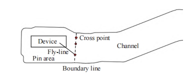
Fig. 1. The demonstration of a part of FPC
In this paper, we propose a bus planning algorithm to improve routability and assign layers while satisfying the special constraints of FPC. First, we construct a pin area interconnection (PAI) model based on the spatial location of the pin, which is essentially an undirected graph, then the dynamic pin sequence (DPS) is used to obtain the topologically non-crossing sequence for the nodes in the PAI model. This sequence is transformed into the order constraint of the crossing point (CP) on the boundary line, and finally a heuristic algorithm is proposed to search the location of the CP. The main contributions of this manuscript are summarized as follows:
● To the best of the authors ’ knowledge, this is the first work to propose a bus planning algorithm for complex FPC.
● Our bus planning generates the CPs on the boundary line, dividing the whole board routing into pin area routing and channel routing, which reduces the solution space and makes it feasible to meet the constraints.
● A heuristic algorithm is used to search the location of the CPs that ensures both the routability of the pin area and the topologically non-crossing constraint of the channel.
● Experimental results show that our method realizes better results in the via count and the routability compared with the current advanced router free-rout-ing.
The rest of this paper is organized as follows. Secion II introduces the preliminaries of our method.Section III introduces the specific optimization algorithm,including topologically non-crossing sequence and CP iterative optimization. Section IV introduces experimental results. Section V concludes the paper.


