- Flex PCB Blog
- PCB Assembly Blog
- FPC Research Blog
- Preparation of FPC based on ultrasonic spraying method_4_Experimental Results
- Preparation of FPC based on ultrasonic spraying method_3_Experimental Procedure
- Preparation of FPC based on ultrasonic spraying method_2_Experimental Platform and Principle
- Preparation of FPC based on ultrasonic spraying method_1_abstract
- Research on Layout Design Method of Ultra-thin FPC_4_Analysis of Layout Design Methods
- Research on Layout Design Method of Ultra-thin FPC_3_Analysis of Layout Design Methods
- Research on Layout Design Method of Ultra-thin FPC_2_Analysis of Layout Design Methods
- Research on Layout Design Method of Ultra-thin FPC_1_introduction
- Research progress on polyimide FPC_2_the field of FPC
- Research progress on polyimide FPC_1_Introduction
- Analysis of Vibration Characteristics of FPCBs _4_Summary
- Analysis of Vibration Characteristics of FPCBs _3_Finite Element Analysis
- Analysis of Vibration Characteristics of FPCBs _2_Theory of Vibration Analysis
- Analysis of Vibration Characteristics of FPCBs Under Random Vibration_1_Introduction
- Design Methods for FPCBs_5_Practical Application
- Design Methods for FPCBs_4_Electrical Circuit Design and Examples
- Design Methods for FPCBs_3_Structure Design Method and Examples
- Design Methods for FPCBs_2_Component Selection Methodology and Examples.
- Research on Design Methods for FPCBs
- Application of MPW technique for FPCBs _4_Summary
- Application of MPW technique for FPCBs_3_Experimental results
- Application of MPW technique for FPCBs_2_Experimental setup
- Application of MPW technique for FPCBs_1_Principle of MPW
- Application of FPCB in PC motherboards_4_ Results and discussion
- Application of FPCB in PC motherboards_3_ Numerical analysis
- Application of FPCB in PC_2_ Experimentation
- Application of FPCB in PC motherboards
- A Bus Planning Algorithm for FPC Design _4_Experimental result
- A Bus Planning Algorithm for FPC Design _3_Proposed Algorithm
- A Bus Planning Algorithm for FPC Design _2_Preliminaries
- A Bus Planning Algorithm for FPC Design _1_Introduction
Research on Layout Design Method of Ultra-thin FPC_4_Analysis of Layout Design Methods
1.3 Mesh Copper Reference Plane EMC Analysis
A large number of existing practices have proven that EMC performance is related to the following two points:
(1) Mesh gap: the smaller the gap, the better the performance.
(2) The copper area of the shielding surface: the larger the area, the better the performance.
From the above, in order to obtain better EMC characteristics, it can be known that:
(1) The smaller the value of Sn in equation (5), the better.
(2) The smaller the value of An in equation (6), the better.
(3) The smaller the duty cycle of the reference mesh surface, the better.
And k=An/Sn. It can be seen from the above that the smaller the value of k, the better the EMC performance. However, in this paper, the value of k has been fixed within a certain range due to the need to ensure the signal integrity of the routing, which is related to the layer spacing of the FPC and is a determined integer, as given in section 1.2. Therefore, the optimal value of k is 4.
The optimization goals are: minimize the value of Sn and minimize the value of An. This paper analyzes different forms of meshes with the same duty cycle.
For the same length of routing, the 45-degree mesh lines as shown in Figure 3(a) have 14 overlaps, while the vertical mesh as shown in Figure 3(b) has 20 overlaps, but the total area of overlap is the same.

(a) 45-degree inclined mesh

(b) Vertical mesh
Figure 3 Two forms of mesh with the same duty cycle
From this, it can be known that the Sn value of the vertical mesh is smaller than that of the 45-degree mesh, with the total area S″ remaining unchanged. It can be inferred that:
With the same duty cycle, the EMC effect of the vertical mesh will be better than that of the 45-degree mesh.
From the above comparison, it can be seen that there is significant room for improvement in the currently common 45-degree mesh copper reference plane design method. Changing the mesh that intersects with the routing at 45 degrees to a mesh perpendicular to the routing can improve the EMC effect.
Additionally, in the aforementioned text, since the value of k is calculated based on the projection area of the routing, it is the duty cycle of a uniform mesh. However, in actual layout design, the duty cycle of the overall mesh reference plane can be reduced. The specific method is: by filling the reference plane projected by the gaps between signal routings with solid copper, that is, filling the non-routing projection area of the mesh reference plane with solid copper. As a result, the overall mesh reference plane becomes a non-uniform mesh, with only the routing projection area being a uniform mesh.
After reducing the overall duty cycle in this way, it does not affect the routing capacitance. But as analyzed earlier, reducing the duty cycle of the overall reference plane can effectively improve EMC performance.
This paper has modeled and simulated this, using a k value of 4.
Specific modeling: FPC layer thickness 0.8 mil; mesh linewidth 5 mil, perpendicular to the routing, mesh gap 20 mil; the non-routing projection area of the mesh reference plane is filled with solid copper. The modeling results are shown in Figure 4(a), and the isolation simulation results of the mesh reference plane are shown in Figure 4(b).
The simulation results show that after the mesh improvement, the shielding isolation of the FPC cable is significantly improved. In Figure 4(b), blue represents the ordinary mesh copper (45-degree inclined mesh, reference plane with uniform mesh), and red represents the improved design method of this paper (vertical mesh, reference plane with non-uniform mesh, only the routing projection area is a uniform mesh).
This simulation result verifies that the research on the design methods of mesh form, mesh size, and mesh proportion of the mesh reference plane in this paper is correct and effective, and can provide a practical and feasible method for the layout design of ultra-thin FPC.
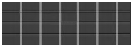
(a) Optimized mesh modeling
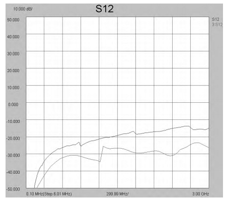
(b) Simulation results after mesh optimization
Figure 4 Optimized modeling and simulation results


