- Flex PCB Blog
- Reflow Soldering PCB Temperature Curve Explanation
- What is FPC
- Special attention points for flexible circuit wiring
- Multilayer PCB Stack-up Basics | PCB Knowledge
- PCB Protection: Potting or Conformal Coating? | PCB Knowledge
- FPCway: Specialized manufacturer of flexible printed circuit boards and rigid-flexible printed circuits
- Future Trends of Flexible Circuit Boards
- Rigid-Flex PCB Stack-up for Impedance Controlled Designs
- Control Impedance Between Rigid PCB and Flex PCB
- Flex PCB Reliability and Bendability
- Normal Flex PCB Specifications
- Flex PCB Polyimide Coverlay and Solder Mask
- Flex PCB Boards and Connectors
- About RA Copper and ED Copper
- Introduction of Flexible PCB
- 5 Tips For Designing Flexible PCB
- Advantages of FPC (Flexible PCB)
- Evolution of the Flex Printed Circuit Board
- Benefits of Using Flex Circuit Boards
- Why Rigid-Flex PCBs are Economical?
- Flexible PCB vs Rigid PCB
- Development of Flexible printed circuit board (FPC) market
- Traditional Manufacture Engineering of FPC Substrate
- Development Trend of FPC Board
- Flex PCB and the Manufacturing
- About Flex PCB design
- About Flex PCB and Assembly
- How to Ensure Flex PCB Design Success
- How to Select the Appropriate FPC Materials?
- The Differences In Rigid PCB, Flex PCB and Rigid-Flex PCB
- Flex-Rigid PCB Design Guidelines
- Beneficials for Polyimide Flex PCB Boards
- About Stiffener on Flex PCB FPC circuit Boards
- About ENIG and ENEPIG
- PCB Surface Finish Comparison
- Copper Thickness for FPC Boards
- Interconnect Solutions for Flexible Printed Circuits and Etched Foil Heaters
- Advantages and Disadvantages of Rigid-Flex PCB
- About FPC Plating Process
- About EMI shield design for Flex Printed Circuit Board
- PCB Assembly Blog
- FPC Research Blog
Impedance controlled circuits in a rigid-flex PCB design is a common requirement throughout the industry in a wide range of applications. Having Impedance control, however, does create an additional challenge for designs that have very demanding minimum bend requirements.
In this blog post, we will review the design and construction specifics of some of the more common rigid-flex circuit board constructions that meet our customers' requirements: impedance-controlled circuit configuration and the impact on flexibility/minimum bend capability, line widths and spacings, materials, copper thickness, and common constructions.
Impedance Controlled Circuit Configuration
By far the most common configurations are the 4 variations of the microstrip and stripline as shown below. These configurations address the needs of 95%+ of all flexible circuit designs that we manufacture.
Embedded Microstrip

Edge Coupled Embedded Microstrip

Symmetrical Stripline

Edge Couple Stripline
Of the two common configurations, the microstrip is the preferred configuration for the flex area of a rigid-flex design. It requires only two flex layers (1 signal layer + 1 reference plane layer) and uses a thinner flex core thickness. This combines to allow for the tightest possible minimum bend radius, which is often necessary to meet the packing requirements of the specific design. This configuration however does not provide shielding against EMI/RF on both sides of the impedance-controlled circuits.
The stripline configuration has the added benefit of providing shield on both sides of the circuitry, however, it has a negative impact on the minimum bend radius capability and flexibility. The required 3-layer construction (1 reference plane + 1 signal layer + 1 reference plane) adds significant thickness to the flex area. In addition, thicker flex cores are needed between the 3 layers to achieve the impedance values. This configuration should only be used if shielding on both sides is a design requirement.
Line Widths/Spacing, Copper Thickness, And Materials
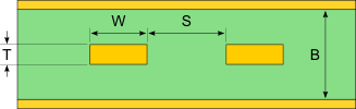
Line widths and spacing, and the copper thickness of the flex layers interact to achieve the impedance values required. Thinner copper allows for a thinner line width/spacing and a thinner flex core thickness. This results in a thinner flex area, which will have the highest degree of flexibility and the tightest min. bend capability.
The preferred copper thickness is ½ OZ copper. Allows for a 0.002”flex core thickness for a microstrip configuration and 0.003” flex cores for a stripline configuration.
The following are typical line widths and spacings for the more common impedance values when using ½ OZ copper:
- 50 Ohm Single Ended: 0.004” line.
- 90 Ohm Differential Pair: 0.004” line/0.0055” spacing.
- 100 Ohm Differential Pair: 0.004” line/0.006” spacing.
- 120 Ohm Differential Pair: 0.0037” line/0.0075” spacing.
If 1 OZ copper is required, usually due to a higher current carrying requirement on non-impedance lines, the above line widths are not valid as a 0.004” line width is below the manufacturable limit of 1 OZ copper. This requires the line widths/spacing as well as the flex core thickness to increase, which negatively impacts flexibility.
Polyimide flex materials are very well suited for impedance-controlled designs. The material is homogenous, has a low DK (3.2-3.4), is very uniform, and has tightly controlled thickness. Polyimide coverlays are also used to encapsulate the flex layers.
Minimum Bend Radius Requirements
All flex designs require the minimum bend requirements of the design to be identified and the materials and construction reviewed to ensure that the finished parts are mechanically reliable when installed. This becomes more important for impedance-controlled designs as the impedance requirement will always require a thicker flex construction.
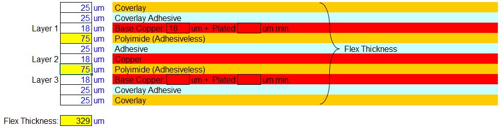
As an example, a standard construction 2-layer flex area utilizing a 0.001” flex core with ½ OZ copper and 0.001” coverlays results in a finished thickness of 0.006” after lamination. Thinner 1/2 mil flex cores and coverlays can be used to reduce the thickness down to as low as 0.004” if needed. An impedance-controlled microstrip configuration, with a 0.002” flex core, increase the flex thickness to 0.007”. A 3-layer stripline significantly increases the flex thickness further to 0.012” due to the added third circuit layer and the increased 2 x 0.003” flex cores.

2-layer standard flex PCB construction

2-layer thin-build flex PCB construction

2-layer microstrip flex PCB construction
3-layer stripline flex PCB construction
Common Rigid-Flex Constructions
Rigid-flex constructions and configurations are available in a very wide variety. The number of combinations is too many to cover within this blog. The following constructions are some of the more commonly used for designs that have an average amount of circuit complexity. For more advanced designs, there are constructions available with higher rigid and/or flex layer counts. For these designs, we recommend to our customers to have a preliminary design review discussion with our engineering team to review the specific routing and bend requirements of the design and from this determine the optimum construction that will meet the design needs.
Application: Connector to connector microstrip impedance control. No active components.
Impedance lines dropped down to the flex layers immediately adjacent to the SMT pads or straight out from PTH connector holes, eliminating need for external layer impedance lines. Additional flex layers available for microstrip configuration if circuit routing exceeds 1 flex layer. The second signal layer need not be impedance-controlled, which allows for second layer flex core thickness reduction and thinner flex section. This is also available with a stripline impedance configuration. It is typically limited to 1 signal layer to prevent excessive flex area thickness.
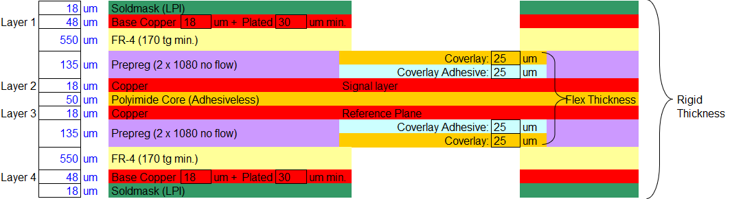
4-layer rigid-flex PCB microstrip construction
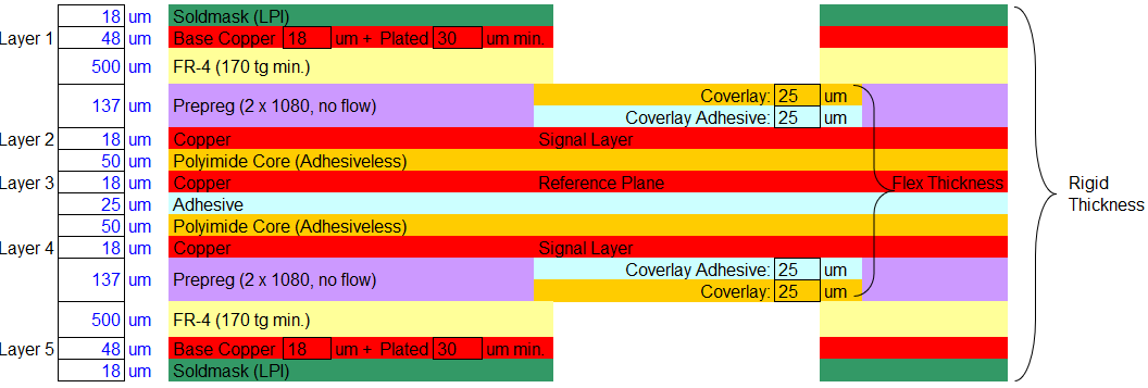
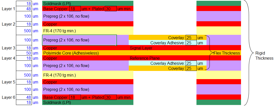
5-layer rigid-flex PCB microstrip construction
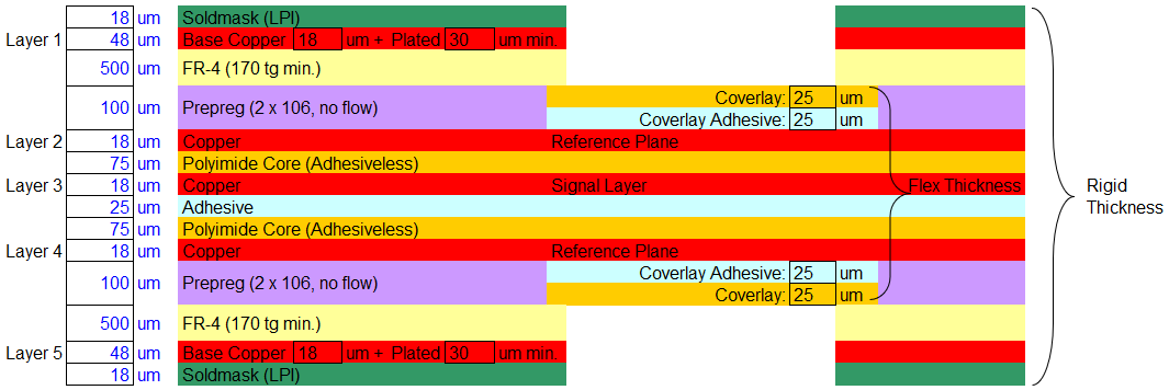
5-layer rigid-flex PCB stripline construction
Application: Active Component Area Rigid Areas.
Active components on one or both rigid circuit board areas that also require Impedance controlled signal routing on external layers. Typically requires a minimum of a 6-layer configuration to allow for additional rigid area reference planes to be located within an effective distance of the external layers and allow for practical Impedance line widths. Flex layer area can be configured as either microstrip or stripline. Microstrip can have additional signal layer if required as per above 5-layer microstrip example.
6-layer rigid-flex PCB stripline construction
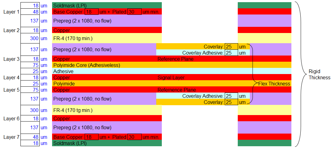
7-layer rigid-flex PCB stripline construction
Summary
Impedance-controlled flexible PCB designs add the requirement of both thicker flex core layers and tightly controlled lines widths and spacing to meet the specific impedance requirements. For the flex areas of a rigid-flex circuit board design, this results in an increase in the flex area thickness, which may then impact the part’s ability to meet the min. bend requirements.
These challenges can be addressed in most designs with a thorough design review and input from an experienced supplier. Please feel free to contact FPCway if you have any questions regarding the design of controlled impedance flexible circuit board.


